- 您现在的位置:买卖IC网 > Sheet目录526 > SUD25N15-52-T4-E3 (Vishay Siliconix)MOSFET N-CH D-S 150V TO252
SUD25N15-52
Vishay Siliconix
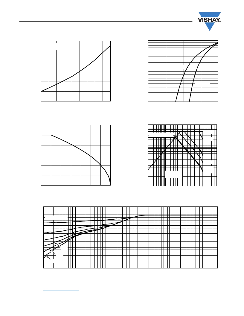
TYPICAL CHARACTERISTICS 25 °C, unless otherwise noted
3.0
2.5
V GS = 10 V
I D = 5 A
100
2.0
T J = 150 °C
1.5
10
1.0
T J = 25 °C
0.5
0.0
1
- 50
- 25
0
25
50
75
100
125
150
175
0
0.3
0.6
0.9
1.2
T J - J u nction Temperat u re ( °C )
On-Resistance vs. Junction Temperature
THERMAL RATINGS
30
100
V SD - So u rce-to-Drain V oltage ( V )
Source-Drain Diode Forward Voltage
25
Limited b y R DS(on) *
10 μ s
100 μ s
20
15
10
10
1
1 ms
10 ms
100 ms
5
T C = 25 °C
Single P u lse
1 s, DC
0
0
25
50 75 100 125
150
175
0.1
0 . 1
1
1 0
100
1 0 0 0
2
1
0.1
T C - Case Temperat u re (°C)
Maximum Avalanche Drain Current
vs. Case Temperature
Duty Cycle = 0.5
0.2
0.1
0.02
0.05
Single Pulse
V DS - Drain-to-So u rce V oltage ( V )
* V GS > minim u m V GS at w hich R DS(on) is specified
Safe Operating Area
0.01
10 -4
10 -3
10 -2
10 -1
1
10
30
Square Wave Pulse Duration (s)
Normalized Thermal Transient Impedance, Junction-to-Case
Vishay Siliconix maintains worldwide manufacturing capability. Products may be manufactured at one of several qualified locations. Reliability data for Silicon
Technology and Package Reliability represent a composite of all qualified locations. For related documents such as package/tape drawings, part marking, and
reliability data, see www.vishay.com/ppg?71768 .
www.vishay.com
4
Document Number: 71768
S09-1501-Rev. D, 10-Aug-09
发布紧急采购,3分钟左右您将得到回复。
相关PDF资料
SUD35N05-26L-E3
MOSFET N-CH D-S 55V TO252
SUD40N02-08-E3
MOSFET N-CH D-S 20V TO252
SUD50N02-09P-E3
MOSFET N-CH D-S 20V DPAK
SUD50N03-06P-E3
MOSFET N-CH D-S 30V TO252
SUD50N03-09P-GE3
MOSFET N-CH D-S 30V TO252
SUD50N03-12P-E3
MOSFET N-CH D-S 30V TO252
SUD50N03-16P-GE3
MOSFET N-CH D-S 30V TO252
SUD50N04-05L-E3
MOSFET N-CH D-S 40V TO252
相关代理商/技术参数
SUD30N03-30
功能描述:MOSFET 30V 30A 50W RoHS:否 制造商:STMicroelectronics 晶体管极性:N-Channel 汲极/源极击穿电压:650 V 闸/源击穿电压:25 V 漏极连续电流:130 A 电阻汲极/源极 RDS(导通):0.014 Ohms 配置:Single 最大工作温度: 安装风格:Through Hole 封装 / 箱体:Max247 封装:Tube
SUD30N03-30
制造商:Vishay Siliconix 功能描述:MOSFET N D-PAK
SUD30N03-30-E3
功能描述:MOSFET 30V 30A 50W RoHS:否 制造商:STMicroelectronics 晶体管极性:N-Channel 汲极/源极击穿电压:650 V 闸/源击穿电压:25 V 漏极连续电流:130 A 电阻汲极/源极 RDS(导通):0.014 Ohms 配置:Single 最大工作温度: 安装风格:Through Hole 封装 / 箱体:Max247 封装:Tube
SUD30N03-30-T4
制造商:Vishay Angstrohm 功能描述:Trans MOSFET N-CH 30V 30A 3-Pin(2+Tab) DPAK T/R
SUD30N04-10
功能描述:MOSFET 40V 30A 97W RoHS:否 制造商:STMicroelectronics 晶体管极性:N-Channel 汲极/源极击穿电压:650 V 闸/源击穿电压:25 V 漏极连续电流:130 A 电阻汲极/源极 RDS(导通):0.014 Ohms 配置:Single 最大工作温度: 安装风格:Through Hole 封装 / 箱体:Max247 封装:Tube
SUD30N04-10-E3
功能描述:MOSFET 40V 30A 97W RoHS:否 制造商:STMicroelectronics 晶体管极性:N-Channel 汲极/源极击穿电压:650 V 闸/源击穿电压:25 V 漏极连续电流:130 A 电阻汲极/源极 RDS(导通):0.014 Ohms 配置:Single 最大工作温度: 安装风格:Through Hole 封装 / 箱体:Max247 封装:Tube
SUD35N05-26L
功能描述:MOSFET 55V 35A 50W RoHS:否 制造商:STMicroelectronics 晶体管极性:N-Channel 汲极/源极击穿电压:650 V 闸/源击穿电压:25 V 漏极连续电流:130 A 电阻汲极/源极 RDS(导通):0.014 Ohms 配置:Single 最大工作温度: 安装风格:Through Hole 封装 / 箱体:Max247 封装:Tube
SUD35N05-26L
制造商:Vishay Siliconix 功能描述:MOSFET N D-PAK
